Loose Leaf for Engineering Circuit Analysis Format: Loose-leaf
9th Edition
ISBN: 9781259989452
Author: Hayt
Publisher: Mcgraw Hill Publishers
expand_more
expand_more
format_list_bulleted
Concept explainers
Videos
Textbook Question
Chapter 5.3, Problem 8P
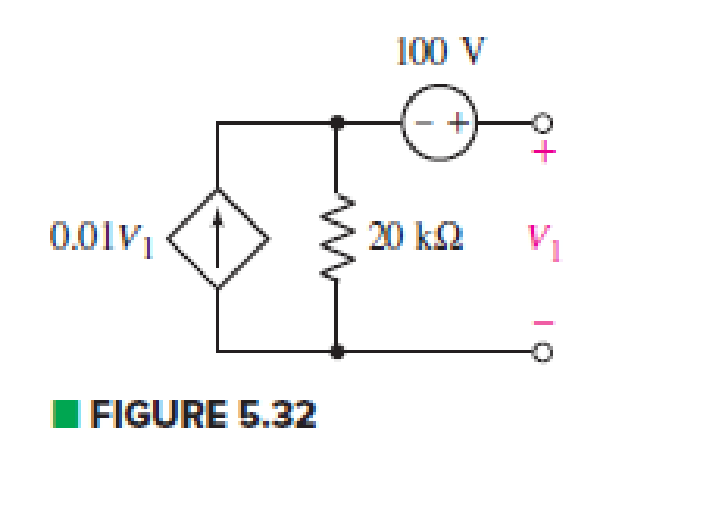
Find the Thévenin equivalent for the network of Fig. 5.32. (Hint: a quick source transformation on the dependent source might help.)
Note: A negative resistance might seem strange—and it is! Such a thing is physically possible only if, for example, we do a bit of clever electronic circuit design to create something that behaves like the dependent current source we represented in Fig. 5.32.
Expert Solution & Answer
Want to see the full answer?
Check out a sample textbook solution
Students have asked these similar questions
A PMMC instruments with FSD=50 micro ampere ,coil resistance 1700 ohm is to be employed as a voltmeter with ranges of 10 V,50 V,100 V ,in circuit using switched ,Calculate the required value of multiplier resistor
3. The network of Figure below is the basic biasing arrangement for the field-effect transistor (FET), a
device of increasing importance in electronic design. (Biasing simply means the application of de
levels to establish a particular set of operating conditions.) Even though you may be unfamiliar with
the FET, you can perform the following analysis using only the basic laws introduced in your lectures
and the information provided on the diagram.
a. Determine the voltages VG and Vs.
b. Find the currents I1, 12, Ip, and Is.
c. Determine VDs.
d. Calculate VDG.
VDD
= 16 V
ID
2 MN
Rp 2.5 kn
R1
오D
VGO
G
= -1.75 V 2l
V s
O's
Is
Ic = 0 A
Ip = Is
R2
270 kn
Rs
1.5 kN
3. The network of Figure below is the basic biasing arrangement for the field-effect transistor (FET), a
device of increasing importance in electronic design. (Biasing simply means the application of de
levels to establish a particular set of operating conditions.) Even though you may be unfamiliar with
the FET, you can perform the following analysis using only the basic laws introduced in your lectures
and the information provided on the diagram.
a. Determine the voltages VG and Vs.
b. Find the currents h, h, In, and Is.
c. Determine Vns.
d. Calculate VDG.
VDD - 16 V
오
2 Mn Ro25 kn
OD
Vas - -1.75 V 4 T
I6 - 0A
In = Is
Ves
o's
R270 kn
Chapter 5 Solutions
Loose Leaf for Engineering Circuit Analysis Format: Loose-leaf
Ch. 5.1 - For the circuit of Fig. 5.4, use superposition to...Ch. 5.2 - For the circuit of Fig. 5.7, use superposition to...Ch. 5.2 - For the circuit of Fig. 5.18, compute the current...Ch. 5.2 - For the circuit of Fig. 5.20, compute the voltage...Ch. 5.3 - Using repeated source transformations, determine...Ch. 5.3 - Use Thvenins theorem to find the current through...Ch. 5.3 - Determine the Thvenin and Norton equivalents of...Ch. 5.3 - Find the Thvenin equivalent for the network of...Ch. 5.3 - Find the Thvenin equivalent for the network of...Ch. 5.4 - Consider the circuit of Fig. 5.43. FIGURE 5.43...
Ch. 5.5 - Prob. 11PCh. 5 - Linear systems are so easy to work with that...Ch. 5 - Prob. 2ECh. 5 - Prob. 3ECh. 5 - (a) Employ superposition to determine the current...Ch. 5 - (a) Using superposition to consider each source...Ch. 5 - (a) Determine the individual contributions of each...Ch. 5 - (a) Determine the individual contributions of each...Ch. 5 - After studying the circuit of Fig. 5.53, change...Ch. 5 - Consider the three circuits shown in Fig. 5.54....Ch. 5 - (a) Using superposition, determine the voltage...Ch. 5 - Employ superposition principles to obtain a value...Ch. 5 - (a) Employ superposition to determine the...Ch. 5 - Perform an appropriate source transformation on...Ch. 5 - (a) For the circuit of Fig. 5.59, plot iL versus...Ch. 5 - Determine the current labeled I in the circuit of...Ch. 5 - Verify that the power absorbed by the 7 resistor...Ch. 5 - (a) Determine the current labeled i in the circuit...Ch. 5 - (a) Using repeated source transformations, reduce...Ch. 5 - Prob. 19ECh. 5 - (a) Making use of repeated source transformations,...Ch. 5 - Prob. 21ECh. 5 - (a) With the assistance of source transformations,...Ch. 5 - For the circuit in Fig. 5.67 transform all...Ch. 5 - Prob. 24ECh. 5 - (a) Referring to Fig. 5.69, determine the Thevenin...Ch. 5 - (a) With respect to the circuit depicted in Fig....Ch. 5 - (a) Obtain the Norton equivalent of the network...Ch. 5 - (a) Determine the Thevenin equivalent of the...Ch. 5 - Referring to the circuit of Fig. 5.71: (a)...Ch. 5 - Prob. 30ECh. 5 - (a) Employ Thvenins theorem to obtain a...Ch. 5 - Prob. 32ECh. 5 - Determine the Norton equivalent of the circuit...Ch. 5 - For the circuit of Fig. 5.75: (a) Employ Nortons...Ch. 5 - (a) Obtain a value for the Thvenin equivalent...Ch. 5 - Prob. 36ECh. 5 - Obtain a value for the Thvenin equivalent...Ch. 5 - With regard to the network depicted in Fig. 5.79,...Ch. 5 - Determine the Thvenin and Norton equivalents of...Ch. 5 - Determine the Norton equivalent of the circuit...Ch. 5 - Prob. 41ECh. 5 - Determine the Thvenin and Norton equivalents of...Ch. 5 - Prob. 43ECh. 5 - Prob. 44ECh. 5 - Prob. 45ECh. 5 - (a) For the simple circuit of Fig. 5.87, find the...Ch. 5 - For the circuit drawn in Fig. 5.88, (a) determine...Ch. 5 - Study the circuit of Fig. 5.89. (a) Determine the...Ch. 5 - Prob. 49ECh. 5 - Prob. 50ECh. 5 - With reference to the circuit of Fig. 5.91, (a)...Ch. 5 - Prob. 52ECh. 5 - Select a value for RL in Fig. 5.93 such that it...Ch. 5 - Determine what value of resistance would absorb...Ch. 5 - Derive the equations required to convert from a...Ch. 5 - Convert the - (or "-") connected networks in Fig....Ch. 5 - Convert the Y-(or T-) connected networks in Fig....Ch. 5 - For the network of Fig. 5.97, select a value of R...Ch. 5 - For the network of Fig. 5.98, select a value of R...Ch. 5 - Prob. 60ECh. 5 - Calculate Rin as indicated in Fig.5.100. FIGURE...Ch. 5 - Employ Y conversion techniques as appropriate to...Ch. 5 - Prob. 63ECh. 5 - (a) Use appropriate techniques to obtain both the...Ch. 5 - (a) For the network in Fig. 5.104, replace the...Ch. 5 - Prob. 66ECh. 5 - Prob. 67ECh. 5 - A 2.57 load is connected between terminals a and...Ch. 5 - A load resistor is connected across the open...Ch. 5 - A backup is required for the circuit depicted in...Ch. 5 - (a) Explain in general terms how source...Ch. 5 - The load resistor in Fig. 5.108 can safely...Ch. 5 - Prob. 74ECh. 5 - As part of a security system, a very thin 100 ...Ch. 5 - With respect to the circuit in Fig. 5.90, (a)...
Knowledge Booster


Learn more about
Need a deep-dive on the concept behind this application? Look no further. Learn more about this topic, electrical-engineering and related others by exploring similar questions and additional content below.Similar questions
- 3. The network of Figure below is the basic biasing arrangement for the field-effect transistor (FET), a device of increasing importance in electronic design. (Biasing simply means the application of de levels to establish a particular set of operating conditions.) Even though you may be unfamiliar with the FET, you can perform the following analysis using only the basic laws introduced in your lectures and the information provided on the diagram. a. Determine the voltages VG and Vs. b. Find the currents I1, I2, ID, and Is. c. Determine Vps. d. Calculate V DG- VDD = 16 V to \ID 32 MN Rp32.5 kN R1 OD VGO Vas = -1.75 V h| IG S VGS IG O's Is = 0 A Ip = Is R2 270 kN %3D Rs 1.5 kNarrow_forward3. The network of Figure below is the basic biasing arrangement for the field-effect transistor (FET), a device of increasing importance in electronic design. (Biasing simply means the application of de levels to establish a particular set of operating conditions.) Even though you may be unfamiliar with the FET, you can perform the following analysis using only the basic laws introduced in your lectures and the information provided on the diagram. a. Determine the voltages Vg and V's. b. Find the currents I1, I2, Ip, and Is. c. Determine Vos. d. Calculate VpG. Vpo = 16 V 오 R1 2 Mn Rp2.5 kn OD VGO Ves = -1.75 V IG - 0A In - Is VGS o's Is IS R2 270 kf Rs 1.5 knarrow_forward3. The network of Figure below is the basic biasing arrangement for the field-effect transistor (FET), a device of increasing importance in electronic design. (Biasing simply means the application of de levels to establish a particular set of operating conditions.) Even though you may be unfamiliar with the FET, you can perform the following analysis using only the basic laws introduced in your lectures and the information provided on the diagram. a. Determine the voltages VG and Vs. b. Find the currents I1, I2, ID, and Is. c. Determine V Ds- d. Calculate VpG- VDD = 16 V 오 ID R1 2 ΜΩ Rp 2.5 kN OD VGO IG VGs = -1.75 V 2 VGS IG = 0 A In = Is o's |Is R2 270 kN Rs 1.5 kNarrow_forward
- 3. The network of Figure below is the basic biasing arrangement for the field-effect transistor (FET), a device of increasing importance in electronic design. (Biasing simply means the application of de levels to establish a particular set of operating conditions.) Even though you may be unfamiliar with the FET, you can perform the following analysis using only the basic laws introduced in your lectures and the information provided on the diagram. a. Determine the voltages VG and Vs. b. Find the currents I1, h, ID, and Is. c. Determine V Ds- d. Calculate VpG- VDD = 16 V ID R 32 MN Rp2.5 kN 오D VGO G I, T VGS as = -1.75 V IG = 0 A Ip = Is oVs R2 270 kN Is Rs 1.5 kNarrow_forward3. The network of Figure below is the basic biasing arrangement for the field-effect transistor (FET), a device of increasing importance in electronic design. (Biasing simply means the application of de levels to establish a particular set of operating conditions.) Even though you may be unfamiliar with the FET, you can perform the following analysis using only the basic laws introduced in your lectures and the information provided on the diagram. a. Determine the voltages VG and Vs. b. Find the currents I1, I2, ID, and Is. c. Determine VDS- d. Calculate DG- VDD = 16 V to ID 2 MN Rp32.5 kN R1 오D VGO VGs = -1.75 V IG = 0 A Ip = Is I IG VGS Is OVs R2 270 k2 Rs 1.5 kNarrow_forward3. The network of Figure below is the basic biasing arrangement for the field-effect transistor (FET), a device of increasing importance in electronic design. (Biasing simply means the application of de levels to establish a particular set of operating conditions.) Even though you may be unfamiliar with the FET, you can perform the following analysis using only the basic laws introduced in your lectures and the information provided on the diagram. a. Determine the voltages VG and Vs. b. Find the currents I1, 2, ID, and Is. c. Determine VDs- d. Calculate VDG- VDD = 16 V 오 ID R1 2 MN RD 2.5 kN 오D VGO VGs = -1.75 V IG = 0A Ip = Is IG VGS Is oVs R2 270 kn Rs 1.5 kNarrow_forward
- Design a DC voltage source to maintain fixed, stable 15 V, 13.6 V and 12.2 V DC voltages to different loads. In order to realize this request, a transformer having a primer voltage 220 V AC and a seconder voltage 27 V AC (220/27 V AC transformer), some silicon diodes, zener diode and some resistors of 1.5 k2 can be considered in design. a) Draw the network b) Explain the tasks of each component and overall operation in your design. c) Calculate load current and power dissipation for zener diodearrow_forward3. The network of Figure below is the basic biasing arrangement for the field-effect transistor (FET), a device of increasing importance in electronic design. (Biasing simply means the application of de levels to establish a particular set of operating conditions.) Even though you may be unfamiliar with the FET, you can perform the following analysis using only the basic laws introduced in your lectures and the information provided on the diagram. a. Determine the voltages VG and Vs. b. Find the currents I1, I2, Ip, and Is. c. Determine Vps. d. Calculate DG- VDD = 16 V ID R1 2 ΜΩ RD 2.5 kN OD VGO VGs = -1.75 V IG = 0 A Ip = Is VGS oVs Is R2 270 kN Rs 1.5 kNarrow_forward2. The ratio arms of the Kelvin bridge of Fig. 5-5 are 100 each. The galvanometer has an internal resistance of 500 and a current sensitivity of 200 mm/μA. The unknown resistance R, = 0.1002 2 and the standard resistance is set at 0.1000 n. A dc current of 10 A is passed through the standard and the unknown from a 2.2- V battery in series with a rheostat. The resistance of the yoke may be neglected. Calculate (a) the deflection of the galvanometer, and (b) the resistance unbalance required to produce a galvanometer deflection of 1 mm. E 2 H R2. in R3 www G Ry R₁ Rx wi Oarrow_forward
- What is the relevance of safety factors in circuit design? Explain in a paragraph with 8 sentences.arrow_forwardDetermine the Equivalent Resistance (Rab) of the circuit. ( please provide illustrations/drawings it is needed for our solutions)arrow_forward3. The network of Figure below is the basic biasing arrangement for the field-effect transistor (FET), a device of increasing importance in electronic design. (Biasing simply means the application of dc levels to establish a particular set of operating conditions.) Even though you may be unfamiliar with the FET, you can perform the following analysis using only the basic laws introduced in your lectures and the information provided on the diagram. a. Determine the voltages VG and Vs. b. Find the currents I1, I2, Ip, and Is. c. Determine VDs. d. Calculate VDG. VDD = 16 V ID R132 MN R25 kN OD IG Vas = -1.75 V 4 Iç = 0A In = Is o's Is R2270 kN Rs1.5 kNarrow_forward
arrow_back_ios
SEE MORE QUESTIONS
arrow_forward_ios
Recommended textbooks for you
 Introductory Circuit Analysis (13th Edition)Electrical EngineeringISBN:9780133923605Author:Robert L. BoylestadPublisher:PEARSON
 Delmar's Standard Textbook Of ElectricityElectrical EngineeringISBN:9781337900348Author:Stephen L. HermanPublisher:Cengage Learning
 Programmable Logic ControllersElectrical EngineeringISBN:9780073373843Author:Frank D. PetruzellaPublisher:McGraw-Hill Education
 Fundamentals of Electric CircuitsElectrical EngineeringISBN:9780078028229Author:Charles K Alexander, Matthew SadikuPublisher:McGraw-Hill Education
 Electric Circuits. (11th Edition)Electrical EngineeringISBN:9780134746968Author:James W. Nilsson, Susan RiedelPublisher:PEARSON
 Engineering ElectromagneticsElectrical EngineeringISBN:9780078028151Author:Hayt, William H. (william Hart), Jr, BUCK, John A.Publisher:Mcgraw-hill Education,
Introductory Circuit Analysis (13th Edition)
Electrical Engineering
ISBN:9780133923605
Author:Robert L. Boylestad
Publisher:PEARSON
Delmar's Standard Textbook Of Electricity
Electrical Engineering
ISBN:9781337900348
Author:Stephen L. Herman
Publisher:Cengage Learning
Programmable Logic Controllers
Electrical Engineering
ISBN:9780073373843
Author:Frank D. Petruzella
Publisher:McGraw-Hill Education
Fundamentals of Electric Circuits
Electrical Engineering
ISBN:9780078028229
Author:Charles K Alexander, Matthew Sadiku
Publisher:McGraw-Hill Education
Electric Circuits. (11th Edition)
Electrical Engineering
ISBN:9780134746968
Author:James W. Nilsson, Susan Riedel
Publisher:PEARSON
Engineering Electromagnetics
Electrical Engineering
ISBN:9780078028151
Author:Hayt, William H. (william Hart), Jr, BUCK, John A.
Publisher:Mcgraw-hill Education,
Z Parameters - Impedance Parameters; Author: Electrical Engineering Authority;https://www.youtube.com/watch?v=qoD4AoNmySA;License: Standard Youtube License