
Loose Leaf for Engineering Circuit Analysis Format: Loose-leaf
9th Edition
ISBN: 9781259989452
Author: Hayt
Publisher: Mcgraw Hill Publishers
expand_more
expand_more
format_list_bulleted
Videos
Textbook Question
Chapter 2, Problem 64E
The network shown in Fig. 2.42 can be used to accurately model the behavior of a bipolar junction transistor provided that it is operating in the forward active mode. The parameter β is known as the current gain. If for this device β = 100, and IB is determined to be 100 μA, calculate (a) IC, the current flowing into the collector terminal, and (b) the power dissipated by the base-emitter region.
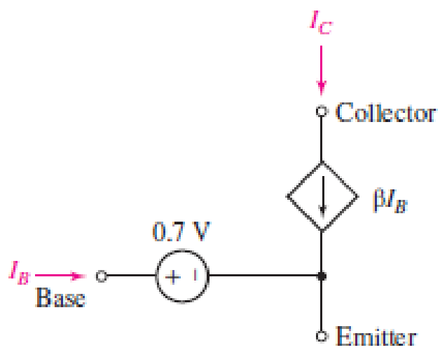
■ FIGURE 2.42 DC model for a bipolar junction transistor operating in forward active mode.
Expert Solution & Answer
Want to see the full answer?
Check out a sample textbook solution
Students have asked these similar questions
NOTE: FOR ALL CIRCUITS SHOWN IN THIS QUIZ ASSUME THAT: β= 100 (for all transistors) ; Early voltage equal to infinity.
1.- In the circuit of figure Nº A, the secondary voltage Vs is 15 volts rms with a frequency of 60 Hz, R equal to 100 Ohms and C equal to 1000 microfarads. The diodes are silicon (Vd = 0.7 volts) and the Zener diode is 15 volts. Determine:a) The magnitude of the ripple voltage at Cb) The Magnitude of the Peak Inverse Voltage (PIV) for D1 and D2
a)
Figure B3 shows a cross section for a Metal Oxide Semiconductor
Field Effect Transistor (MOSFET) in diagrammatic form.
(i)
(ii)
Sketch the energy band diagram for the MOSFET along the
line X-Y shown in Figure B3 when bias voltages are applied
such that the silicon surface is inverted. Label all important
features of your sketch and state any assumptions made.
Sketch a box plot showing the charges present in the structure
when the silicon surface is inverted. Indicate the source of all
the charges and state whether they are positive or negative.
Source n+
Metal
Silicon
Substrate - p
X
dioxide
Drain n*
Q1) Answer True or False for the following:
1- Field-effect transistors are Bipolar devices.
2- A depletion MOSFET (D-MOSFET) can operate with a zero, positive, or negative gate-to
source voltage.
3- The 4-layer diode is a thyristor that conducts when the voltage across its terminals
exceeds the breakover potential.
4- The benefit of SCR Crowbar is power amplification.
5- Most op-amps require only a positive dc supply voltage.
Chapter 2 Solutions
Loose Leaf for Engineering Circuit Analysis Format: Loose-leaf
Ch. 2.1 - A krypton fluoride laser emits light at a...Ch. 2.1 - A typical incandescent reading lamp runs at 60 W....Ch. 2.2 - In the wire of Fig. 2.7, electrons are moving left...Ch. 2.2 - For the element in Fig. 2.11, v1 = 17 V. Determine...Ch. 2.2 - Prob. 6PCh. 2.2 - Determine the power being generated by the circuit...Ch. 2.2 - Determine the power being delivered to the circuit...Ch. 2.2 - Your rechargeable smartphone battery has a voltage...Ch. 2.3 - Find the power absorbed by each element in the...Ch. 2.4 - Prob. 11P
Ch. 2.4 - Prob. 12PCh. 2.4 - The power absorbed by the resistor if i = 3 nA and...Ch. 2 - Convert the following to engineering notation: (a)...Ch. 2 - Convert the following to engineering notation:...Ch. 2 - Prob. 3ECh. 2 - Prob. 4ECh. 2 - Convert the following to SI units, taking care to...Ch. 2 - Prob. 6ECh. 2 - It takes you approximately 2 hours to finish your...Ch. 2 - A certain krypton fluoride laser generates 15 ns...Ch. 2 - Your recommended daily food intake is 2500 food...Ch. 2 - An electric vehicle is driven by a single motor...Ch. 2 - Under insolation conditions of 500 W/m2 (direct...Ch. 2 - A certain metal oxide nanowire piezoelectricity...Ch. 2 - Assuming a global population of 9 billion people,...Ch. 2 - The total charge flowing out of one end of a small...Ch. 2 - Prob. 15ECh. 2 - The total charge stored on a 1 cm diameter...Ch. 2 - A mysterious device found in a forgotten...Ch. 2 - A new type of device appears to accumulate charge...Ch. 2 - The current flowing through a tungsten-filament...Ch. 2 - The current waveform depicted in Fig. 2.28 is...Ch. 2 - The current waveform depicted in Fig. 2.29 is...Ch. 2 - A wind power system with increasing windspeed has...Ch. 2 - Two metallic terminals protrude from a device. The...Ch. 2 - The convention for voltmeters is to use a black...Ch. 2 - Determine the power absorbed by each of the...Ch. 2 - Determine the power absorbed by each of the...Ch. 2 - Determine the unknown current for the circuit in...Ch. 2 - A constant current of 1 ampere is measured flowing...Ch. 2 - Determine the power supplied by the leftmost...Ch. 2 - The currentvoltage characteristic of a silicon...Ch. 2 - A particular electric utility charges customers...Ch. 2 - The Tilting Windmill Electrical Cooperative LLC...Ch. 2 - A laptop computer consumes an average power of 20...Ch. 2 - You have just installed a rooftop solar...Ch. 2 - Prob. 35ECh. 2 - Some of the ideal sources in the circuit of Fig....Ch. 2 - Prob. 37ECh. 2 - Refer to the circuit represented in Fig. 2.35,...Ch. 2 - Prob. 39ECh. 2 - Prob. 40ECh. 2 - Prob. 41ECh. 2 - Determine the magnitude of the current flowing...Ch. 2 - Real resistors can only be manufactured to a...Ch. 2 - (a) Sketch the current-voltage relationship...Ch. 2 - Prob. 45ECh. 2 - Figure 2.38 depicts the currentvoltage...Ch. 2 - Examine the I-V characteristics in Fig. 2.38....Ch. 2 - Determine the conductance (in siemens) of the...Ch. 2 - Determine the magnitude of the current flowing...Ch. 2 - A 1% tolerance 1 k resistor may in reality have a...Ch. 2 - Utilize the fact that in the circuit of Fig. 2.39,...Ch. 2 - For the circuit in Fig. 2.39, suppose that the...Ch. 2 - For each of the circuits in Fig. 2.40, find the...Ch. 2 - Sketch the power absorbed by a 100 resistor as a...Ch. 2 - You built an android that has a subcircuit...Ch. 2 - Using the data in Table 2.4, calculate the...Ch. 2 - Prob. 58ECh. 2 - Prob. 59ECh. 2 - Prob. 60ECh. 2 - The resistance values in Table 2.4 are calibrated...Ch. 2 - Prob. 62ECh. 2 - Prob. 63ECh. 2 - The network shown in Fig. 2.42 can be used to...Ch. 2 - Prob. 65ECh. 2 - An LED operates at a current of 40 mA, with a...Ch. 2 - You have found a way to directly power your wall...
Knowledge Booster


Learn more about
Need a deep-dive on the concept behind this application? Look no further. Learn more about this topic, electrical-engineering and related others by exploring similar questions and additional content below.Similar questions
- 21. The below picture shows a complete npn transistor. In creating this transistor, silicon doped with phosphorus is made into a polished wafer first. What is the next step in the manufacturing process? ➤ a. Doping with a p type chemical b. Etching c. Growing the SiO2 layer d. Apply photoresist n nt Р n Al SiO₂ narrow_forwardAn intrinsic semiconductor is neither a good conductor nor a good insulator. Select one: True False If the value of dc alpha is 0.5, then the value of dc beta of a transistor is O 100 1 O 0.1 O 10 Clear my choice The peak inverse voltage or PIV for the bridge rectifier is lower when compared to an identical center tapped rec Select one: O True O Falsearrow_forwardQuestions One Consider a uniformly doped silicon bipolar transistor at T=300K with a base doping of N, =5 x 10" cm' and collector doping of 2 x 10 cm. Assume the metallurgical base width is 70um. Calculate the change in neutral base width at the C-B voltage of 2V. (Hint Calculate depletion width to the base side at V = 2V and subtract for original length)arrow_forward
- In npn(bipolar junction transistor), the number of charge carriers in the base is more than the emitter. True False . A Moving to another question will save this response.arrow_forwardConsider the two devices shaun below which are fabricated from the semiconductor material. same i) ii) p-type metal n-tmpe Metal metel n-pe metal than ncident on b) if the metal contects across the device is connected with a wire, do you expect current flow hE any ii). in device i) and Explain in te werds each.arrow_forward1- Within the PN-junction, one of the following is not moving:_ A) majority carriers B) ions C) holes D) free electrons 2- Ionization in the semiconductor PN junction creates a layer on each side of the junction line called the A) junction B) depletion region C) barrier voltage D) forward voltage 3- The depletion layer is created due to A) doping B) diffusion C) barrier potential D) ions 4- Silicone atoms are combined into a shape called A) covalent bond B) crystal C) semiconductor D) valence orbit 5) In N-type semiconductor the majority carriers are A) holes B) dopants C) slower D) electrons 6- The PN-junction material can be used to sense A) magnetism B) temperature C) pressure D) all of the abovearrow_forward
- A hole and electron in close proximity would tend to a. Repel each other b. Attract each other C. Have no effect on each other d. None of the above In a semiconductor, current conduction is due to a. Only holes b. Only free electrons c. Holes and free electrons d. None of the above The battery connections required to reverse bias a pn junction are a. +ve terminal to p and -ve terminal to n b. -ve terminal to p and +ve terminal to n c. -ve terminal to p and -ve terminal to n d. None of the abovearrow_forward(b) Figure 2.3 shows the bipolar junction transistor (BJT) voltage divider bias circuit. Determine the value of Ic, VE, VB, VCE, VBC and R1. Given the parameter of the transistor B = 80 and VBE = 0.7V. %3D 18 V 4.7 k2 R1 Ic OVc = 12 V VB o VE 5.6 kN 1.2 k2 Figure 2.3arrow_forwardDerive the current equations for the circuit shown below, using the labels as shown.Note that rz here is a model of the parasitic imperfection of the Zener diode.a) IL = ?b) II = ?c) IZ = ?d) What impact does rz have on VL?arrow_forward
- 2. We discussed in class how the channel capacitance can be modeled in different region of operations in MOSFETs. For your reference, the slide is shown below. Explain how you think the model would look like if a transistor is in velocity saturation region? Channel Capacitances Channel capacitance is a voltage dependent and non-linear capacitance S C P-sub Bulk Cutoff Region D Operation Region Cutoff Linear Saturation S P-sub Bulk C Linear Region CGBCH CoxWLeff 0 0 1 2 3 S P-sub Bulk Saturation Region CGSCH 0 сат CoxWL eff 1 2 CGDCH 0 CoxWLoft CoxWLoff eff D 0arrow_forwardFor the circuit shown find: a. Power consumed in RL b. DC voltage of current source Ip dc. c. Q points of operation of the 2 transistors If it is not possible to calculate explain by laws. ID = 3 milliamperes. All semiconductors are silicon. Vcc 12 V BETA=100 ID Q1 D1 D2 Q2 100 Q D, 10 k2 VEE - 12 Varrow_forwardProblem 2. In a typical MOSFET structure with a p-Si body, the Drain/Body and Source/Body regions are comprised of pn- junction diodes because the Drain and Source electrodes are attached to the p-Si body layer through a small island-like region of n-Si. If these n-Si regions were not present, describe what would happen if you tried to measure the channel current between the Source and Drain electrodes in this device (assuming the gate voltage has properly created an inversion channel)?arrow_forward
arrow_back_ios
SEE MORE QUESTIONS
arrow_forward_ios
Recommended textbooks for you
 Introductory Circuit Analysis (13th Edition)Electrical EngineeringISBN:9780133923605Author:Robert L. BoylestadPublisher:PEARSON
 Delmar's Standard Textbook Of ElectricityElectrical EngineeringISBN:9781337900348Author:Stephen L. HermanPublisher:Cengage Learning
 Programmable Logic ControllersElectrical EngineeringISBN:9780073373843Author:Frank D. PetruzellaPublisher:McGraw-Hill Education
 Fundamentals of Electric CircuitsElectrical EngineeringISBN:9780078028229Author:Charles K Alexander, Matthew SadikuPublisher:McGraw-Hill Education
 Electric Circuits. (11th Edition)Electrical EngineeringISBN:9780134746968Author:James W. Nilsson, Susan RiedelPublisher:PEARSON
 Engineering ElectromagneticsElectrical EngineeringISBN:9780078028151Author:Hayt, William H. (william Hart), Jr, BUCK, John A.Publisher:Mcgraw-hill Education,
Introductory Circuit Analysis (13th Edition)
Electrical Engineering
ISBN:9780133923605
Author:Robert L. Boylestad
Publisher:PEARSON
Delmar's Standard Textbook Of Electricity
Electrical Engineering
ISBN:9781337900348
Author:Stephen L. Herman
Publisher:Cengage Learning
Programmable Logic Controllers
Electrical Engineering
ISBN:9780073373843
Author:Frank D. Petruzella
Publisher:McGraw-Hill Education
Fundamentals of Electric Circuits
Electrical Engineering
ISBN:9780078028229
Author:Charles K Alexander, Matthew Sadiku
Publisher:McGraw-Hill Education
Electric Circuits. (11th Edition)
Electrical Engineering
ISBN:9780134746968
Author:James W. Nilsson, Susan Riedel
Publisher:PEARSON
Engineering Electromagnetics
Electrical Engineering
ISBN:9780078028151
Author:Hayt, William H. (william Hart), Jr, BUCK, John A.
Publisher:Mcgraw-hill Education,
How a MOSFET Works - with animation! | Intermediate Electronics; Author: CircuitBread;https://www.youtube.com/watch?v=Bfvyj88Hs_o;License: Standard Youtube License