
Videos
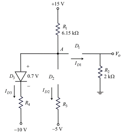
The cut−in voltage of each diode in the circuit shown in Figure P2.52 is
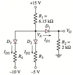
Figure P2.52
(a)
The values of
Answer to Problem 2.52P
The current flowing through diodes is
Explanation of Solution
Given:
Calculation:
The cut-in voltage for each diode is,
Assume all diodes are ON.
Draw the circuit diagram with node voltages and cut-in voltages.
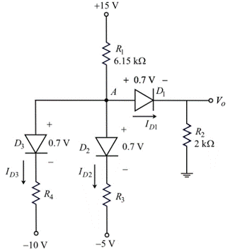
Apply Kirchhoff’s current law node A.
Substitute
Therefore, the voltage at node
Calculate the current flowing through diode,
Substitute
Therefore, the current flowing through diode
Calculate the current flowing through diode,
Substitute
Therefore, the current flowing through diode
Calculate the current flowing through diode,
Substitute
Therefore, the current flowing through diodes is
Conclusion:
Therefore, the current flowing through diodes is
(b)
The values of
Answer to Problem 2.52P
The current flowing through diodes is
Explanation of Solution
Given:
Calculation:
Assume diode
Draw the circuit diagram with node voltages and cut-in voltages.
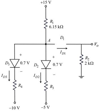
Apply Kirchhoff’s current law node A.
Substitute
Therefore, the voltage at node
The diode
That is,
Therefore, the current flowing through diode
Calculate the current flowing through diode,
Substitute
Therefore, the current flowing through diode
Calculate the current flowing through diode,
Substitute
Therefore, the current flowing through diode
Conclusion:
Therefore, the current flowing through diodes is
(c)
The values of
Answer to Problem 2.52P
The current flowing through diodes is
Explanation of Solution
Given:
Calculation:
Assume diode
Draw the circuit diagram with node voltages and cut-in voltages.
Apply Kirchhoff’s current law node A.
Substitute
Therefore, the voltage at node
The Diode
That is,
Therefore, the current flowing through diode
The current flowing through the diode,
That is,
Therefore, the current flowing through diode
Calculate the current flowing through diode,
Substitute
Therefore, the current flowing through diode
Conclusion:
Therefore, the current flowing through diodes is
Want to see more full solutions like this?
Chapter 2 Solutions
Microelectronics: Circuit Analysis and Design


 Introductory Circuit Analysis (13th Edition)Electrical EngineeringISBN:9780133923605Author:Robert L. BoylestadPublisher:PEARSON
 Delmar's Standard Textbook Of ElectricityElectrical EngineeringISBN:9781337900348Author:Stephen L. HermanPublisher:Cengage Learning
 Programmable Logic ControllersElectrical EngineeringISBN:9780073373843Author:Frank D. PetruzellaPublisher:McGraw-Hill Education
 Fundamentals of Electric CircuitsElectrical EngineeringISBN:9780078028229Author:Charles K Alexander, Matthew SadikuPublisher:McGraw-Hill Education
 Electric Circuits. (11th Edition)Electrical EngineeringISBN:9780134746968Author:James W. Nilsson, Susan RiedelPublisher:PEARSON
 Engineering ElectromagneticsElectrical EngineeringISBN:9780078028151Author:Hayt, William H. (william Hart), Jr, BUCK, John A.Publisher:Mcgraw-hill Education,