Microelectronics: Circuit Analysis and Design
4th Edition
ISBN: 9780073380643
Author: Donald A. Neamen
Publisher: McGraw-Hill Companies, The
bartleby

Videos

Question
Book Icon
Chapter 12, Problem 12.40P

(a)

To determine

Value of current IDQ1 and ICQ2 .

(a)

Expert Solution
Check Mark

Answer to Problem 12.40P

Value of current is,

  IDQ1=0.4056mAICQ2=0.83mA

Explanation of Solution

Given:

The given values are:

  V+=5VVGG=2.5VRD1=5RE2=1.6RL=1.2Kn=1.5(mAV2)VTN=0.5Vλ=0hFE=120VEB(on)=0.7VVA=

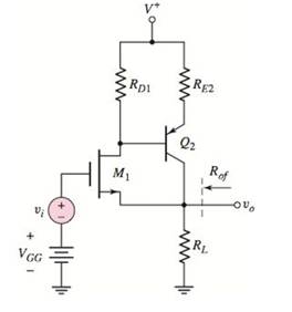
The given circuit is shown below.

  Microelectronics: Circuit Analysis and Design, Chapter 12, Problem 12.40P , additional homework tip  1

Calculation:

Modified circuit diagram is shown below.

  Microelectronics: Circuit Analysis and Design, Chapter 12, Problem 12.40P , additional homework tip  2

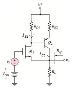
Neglecting base current.

Equation of current ID1 is,

  ID1=5VDRD1ID1=5VD5(1)

Equation of voltage VD is,

  VD=55ID1(2)

Equation of current IC2 is,

  IC2=5(VD+0.7)RE2IC2=4.3VD1.6(3)

Value of voltage VGS is,

  Usingequation(2)IC2=4.3(55ID1)1.6IC2=0.4375+3.125ID1(4)ID1+IC2=VGGVGSRLUsingequation(4)ID10.4375+3.125ID1=2.5VGS1.24.95ID1=3.025VGSVGS=3.0254.95Kn(VGS0.5)2VGS=3.0254.95×1.5(VGS0.5)27.425VGS26.425VGS1.16875=0VGS=(6.425)±(6.425)24×7.425×1.168752×7.425VGS=1.02V

Value of current IDQ1 is,

  IDQ1=Kn(VGS0.5)2IDQ1=1.5(1.020.5)2IDQ1=0.4056mA

Value of current ICQ2 is,

  ICQ2=0.4375+3.125ID1ICQ2=0.4375+3.125×0.4056ICQ2=0.83mA

(b)

To determine

Value of small signal voltage gain.

(b)

Expert Solution
Check Mark

Answer to Problem 12.40P

Value of small signal voltage gain is 0.88.

Explanation of Solution

Given:

Given values are:

  V+=5VVGG=2.5VRD1=5RE2=1.6RL=1.2Kn=1.5(mAV2)VTN=0.5Vλ=0hFE=120VEB(on)=0.7VVA=IDQ1=0.4056mAICQ2=0.83mA

Calculation:

Small signal circuit is shown below.

  Microelectronics: Circuit Analysis and Design, Chapter 12, Problem 12.40P , additional homework tip  3

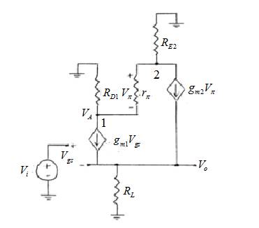
Value of trans-conductance of transistor 1 is,

  gm1=2KnID1gm1=21.5×0.4056gm1=1.56(mA/V)

Value of trans-conductance of transistor 2,

  gm2=IC2VTgm2=0.830.026gm2=31.92(mA/V)

Value of small signal resistance is,

  rπ2=βVTIC2rπ2=120×0.0260.83rπ2=3.759

Applying KCL at node (2),

  VA+VπRE2+Vπrπ+gm2Vπ=0VA1.6=Vπ(11.6+13.759+31.92)VA=52.49Vπ(1)

Equation of output voltage is,

  Vo=(gm1Vgs+gm2Vπ)RL(2)

Applying KCL at node (1),

  VARD1+gm1Vgs=VπrπUsingequation(1)52.49Vπ5+1.56Vgs=Vπ3.759Vgs=6.944Vπ(3)Vπ=0.144VgsUsingequation(Vgs=ViVo)Vπ=0.144(ViVo)(4)

Value of small signal voltage gain is,

  Usingequation(3)and(4)inequation(2).Vo=(1.56×6.944×0.144(ViVo)+31.92×0.144(ViVo))×1.2Vo=1.87(ViVo)+5.51(ViVo)Vo+1.87Vo+5.51Vo=1.87Vi+5.51ViVoVi=0.88

(c)

To determine

Value of small signal output resistance.

(c)

Expert Solution
Check Mark

Answer to Problem 12.40P

Value of small signal output resistance is 143 Ω .

Explanation of Solution

Given:

Given values are,

  V+=5VVGG=2.5VRD1=5RE2=1.6RL=1.2Kn=1.5(mAV2)VTN=0.5Vλ=0hFE=120VEB(on)=0.7VVA=IDQ1=0.4056mAICQ2=0.83mA

Calculation:

Small signal circuit for output resistance calculation ( Vi =0) is,

  Microelectronics: Circuit Analysis and Design, Chapter 12, Problem 12.40P , additional homework tip  4

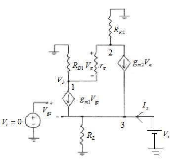
Applying KCL at node 3 for output resistance,

  Ix+gm2Vπ+gm1Vgs=VxRLUsingequation(Vx=VgsVπ=0.144Vgs=0.144Vx)Ix=31.92×0.144Vx(1.56×Vx)+Vx1.2Ro=VxIx=143Ω

Want to see more full solutions like this?

Subscribe now to access step-by-step solutions to millions of textbook problems written by subject matter experts!
Students have asked these similar questions
RDI U₁ Roz M₁ +24V 15M3 2.5 mA 1.3 mA -02041 -24V RDI N2 On the left is a two-stage MOSFET differential amplifier. Note that the second stage still takes in the differential input. Assume the current sources are ideal. The transistor parameters are K₁ = 0.2mA/V², VTN = 2V, and λ = 0.02V-¹ (a) Design the circuit such that vo1 = V02 = 3.3V and Vo4 = 5V when v₁ = V₂ = 0 (b) Determine the differential gain of the first stage, Adı = P01-Voz va V04 (c) Determine the overall differential gain, Ad = vd
Hello! Please show all work, and please show verification for the triodes mode as explained at the bottom, thank you in advance :)
(a) Perform a Monte Carlo analysis of the six-stage cascade amplifier design resulting from the exam- ple in Tables 12.4 and 12.5, and determine the frac- tion of the amplifiers that will not meet either the gain or bandwidth specifications. Assume the resis- tors are uniformly distributed between their limits. A, > 100 dB fu 2 50 kHz and (b) What tolerance must be used to ensure that less than 0.1 percent of the amplifiers fail to meet both specifications? The equation here can be used to estimate the location of the half-power frequency for N closely spaced poles, where fHi is the average of the indi- vidual cutoff frequencies of the N stages and f is the cutoff frequency of the ith individual stage. fH = FHIV2/N – 1 where THi =E fin n

Chapter 12 Solutions

Microelectronics: Circuit Analysis and Design

Ch. 12 - Prob. 12.5TYUCh. 12 - Consider the noninverting op-amp circuit shown in...Ch. 12 - Design a feedback voltage amplifier to provide a...Ch. 12 - Prob. 12.6TYUCh. 12 - (a) Assume the transistor in the source-follower...Ch. 12 - Consider the common-base circuit in Figure...Ch. 12 - Design a feedback current amplifier to provide a...Ch. 12 - Prob. 12.8TYUCh. 12 - Prob. 12.9TYUCh. 12 - For the circuit in Figure 12.31, the transistor...Ch. 12 - Design a transconductance feedback amplifier with...Ch. 12 - Prob. 12.10TYUCh. 12 - Consider the circuit in Figure 12.39, with...Ch. 12 - Consider the BJT feedback circuit in Figure...Ch. 12 - Prob. 12.12TYUCh. 12 - Consider the circuit in Figure...Ch. 12 - Prob. 12.16EPCh. 12 - Prob. 12.17EPCh. 12 - Consider the circuit in Figure 12.44(a) with...Ch. 12 - Consider the circuit in Figure 12.16 with the...Ch. 12 - Prob. 12.18EPCh. 12 - Consider the loop gain function T(f)=(3000)(1+jf...Ch. 12 - Consider the loop gain function given in Exercise...Ch. 12 - Prob. 12.16TYUCh. 12 - Prob. 12.17TYUCh. 12 - Prob. 12.20EPCh. 12 - Prob. 12.21EPCh. 12 - Prob. 12.22EPCh. 12 - What are the two general types of feedback and...Ch. 12 - Prob. 2RQCh. 12 - Prob. 3RQCh. 12 - Prob. 4RQCh. 12 - Prob. 5RQCh. 12 - Prob. 6RQCh. 12 - Describe the series and shunt output connections...Ch. 12 - Describe the effect of a series or shunt input...Ch. 12 - Describe the effect of a series or shunt output...Ch. 12 - Consider a noninverting op-amp circuit. Describe...Ch. 12 - Prob. 11RQCh. 12 - What is the Nyquist stability criterion for a...Ch. 12 - Using Bode plots, describe the conditions of...Ch. 12 - Prob. 14RQCh. 12 - Prob. 15RQCh. 12 - Prob. 16RQCh. 12 - Prob. 17RQCh. 12 - (a) A negative-feedback amplifier has a...Ch. 12 - Prob. 12.2PCh. 12 - The ideal feedback transfer function is given by...Ch. 12 - Prob. 12.4PCh. 12 - Consider the feedback system shown in Figure 12.1...Ch. 12 - The open-loop gain of an amplifier is A=5104. If...Ch. 12 - Two feedback configurations are shown in Figures...Ch. 12 - Three voltage amplifiers are in cascade as shown...Ch. 12 - (a) The open-loop low-frequency voltage gain of an...Ch. 12 - (a) Determine the closed-loop bandwidth of a...Ch. 12 - (a) An inverting amplifier uses an op-amp with an...Ch. 12 - The basic amplifier in a feedback configuration...Ch. 12 - Consider the two feedback networks shown in...Ch. 12 - Prob. 12.14PCh. 12 - Two feedback configurations are shown in Figures...Ch. 12 - Prob. 12.16PCh. 12 - The parameters of the ideal series-shunt circuit...Ch. 12 - For the noninverting op-amp circuit in Figure...Ch. 12 - Consider the noninverting op-amp circuit in Figure...Ch. 12 - The circuit parameters of the ideal shunt-series...Ch. 12 - Consider the ideal shunt-series amplifier shown in...Ch. 12 - Consider the op-amp circuit in Figure P12.22. The...Ch. 12 - An op-amp circuit is shown in Figure P12.22. Its...Ch. 12 - Prob. 12.24PCh. 12 - Prob. 12.25PCh. 12 - Consider the circuit in Figure P12.26. The input...Ch. 12 - The circuit shown in Figure P12.26 has the same...Ch. 12 - The circuit parameters of the ideal shunt-shunt...Ch. 12 - Prob. 12.29PCh. 12 - Consider the current-to-voltage converter circuit...Ch. 12 - Prob. 12.31PCh. 12 - Determine the type of feedback configuration that...Ch. 12 - Prob. 12.33PCh. 12 - A compound transconductance amplifier is to be...Ch. 12 - The parameters of the op-amp in the circuit shown...Ch. 12 - Prob. 12.36PCh. 12 - Consider the series-shunt feedback circuit in...Ch. 12 - The circuit shown in Figure P12.38 is an ac...Ch. 12 - Prob. 12.39PCh. 12 - Prob. 12.40PCh. 12 - Prob. 12.41PCh. 12 - Prob. 12.42PCh. 12 - Prob. D12.43PCh. 12 - Prob. D12.44PCh. 12 - An op-amp current gain amplifier is shown in...Ch. 12 - Prob. 12.46PCh. 12 - Prob. 12.47PCh. 12 - Prob. 12.48PCh. 12 - The circuit in Figure P 12.49 has transistor...Ch. 12 - (a) Using the small-signal equivalent circuit in...Ch. 12 - The circuit in Figure P12.51 is an example of a...Ch. 12 - Prob. 12.52PCh. 12 - For the transistors in the circuit in Figure P...Ch. 12 - Consider the transconductance amplifier shown in...Ch. 12 - Consider the transconductance feedback amplifier...Ch. 12 - Prob. 12.57PCh. 12 - Prob. D12.58PCh. 12 - Prob. 12.59PCh. 12 - Prob. D12.60PCh. 12 - Prob. 12.61PCh. 12 - The transistor parameters for the circuit shown in...Ch. 12 - Prob. 12.63PCh. 12 - For the circuit in Figure P 12.64, the transistor...Ch. 12 - Prob. 12.65PCh. 12 - Prob. 12.66PCh. 12 - Design a feedback transresistance amplifier using...Ch. 12 - Prob. 12.68PCh. 12 - Prob. 12.69PCh. 12 - Prob. 12.70PCh. 12 - The transistor parameters for the circuit shown in...Ch. 12 - Prob. 12.72PCh. 12 - The open-loop voltage gain of an amplifier is...Ch. 12 - A loop gain function is given by T(f)=( 103)(1+jf...Ch. 12 - A three-pole feedback amplifier has a loop gain...Ch. 12 - A three-pole feedback amplifier has a loop gain...Ch. 12 - A feedback system has an amplifier with a...Ch. 12 - Prob. 12.78PCh. 12 - Prob. 12.79PCh. 12 - Consider a feedback amplifier for which the...Ch. 12 - Prob. 12.81PCh. 12 - A feedback amplifier has a low-frequency open-loop...Ch. 12 - Prob. 12.83PCh. 12 - A loop gain function is given by T(f)=500(1+jf 10...Ch. 12 - Prob. 12.85PCh. 12 - Prob. 12.86PCh. 12 - Prob. 12.87PCh. 12 - Prob. 12.88PCh. 12 - The amplifier described in Problem 12.82 is to be...Ch. 12 - Prob. 12.90PCh. 12 - Prob. 12.91CSPCh. 12 - Prob. 12.93CSPCh. 12 - Prob. 12.94CSPCh. 12 - Prob. D12.95DPCh. 12 - Op-amps with low-frequency open-loop gains of 5104...Ch. 12 - Prob. D12.97DP
Knowledge Booster
Background pattern image
Electrical Engineering
Learn more about
Need a deep-dive on the concept behind this application? Look no further. Learn more about this topic, electrical-engineering and related others by exploring similar questions and additional content below.
Similar questions
SEE MORE QUESTIONS
Recommended textbooks for you
Text book image
Introductory Circuit Analysis (13th Edition)
Electrical Engineering
ISBN:9780133923605
Author:Robert L. Boylestad
Publisher:PEARSON
Text book image
Delmar's Standard Textbook Of Electricity
Electrical Engineering
ISBN:9781337900348
Author:Stephen L. Herman
Publisher:Cengage Learning
Text book image
Programmable Logic Controllers
Electrical Engineering
ISBN:9780073373843
Author:Frank D. Petruzella
Publisher:McGraw-Hill Education
Text book image
Fundamentals of Electric Circuits
Electrical Engineering
ISBN:9780078028229
Author:Charles K Alexander, Matthew Sadiku
Publisher:McGraw-Hill Education
Text book image
Electric Circuits. (11th Edition)
Electrical Engineering
ISBN:9780134746968
Author:James W. Nilsson, Susan Riedel
Publisher:PEARSON
Text book image
Engineering Electromagnetics
Electrical Engineering
ISBN:9780078028151
Author:Hayt, William H. (william Hart), Jr, BUCK, John A.
Publisher:Mcgraw-hill Education,
Diode Logic Gates - OR, NOR, AND, & NAND; Author: The Organic Chemistry Tutor;https://www.youtube.com/watch?v=9lqwSaIDm2g;License: Standard Youtube License